Table of Contents
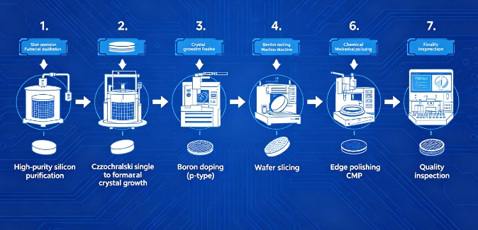
The p-type silicon wafer is one of the most widely utilized foundational materials in the semiconductor industry, playing a critical role in powering modern electronic devices and renewable energy systems. By introducing boron as a dopant into high-purity silicon, p-type wafers create positive charge carriers that enable controlled electrical conductivity. Due to its mature manufacturing process, stable performance, and cost efficiency, the p-type silicon wafer is extensively applied across various technological fields. From consumer electronics to solar energy systems and industrial devices, it serves as a core material that supports the development of modern digital infrastructure.
Application in Integrated Circuits and Consumer Electronics
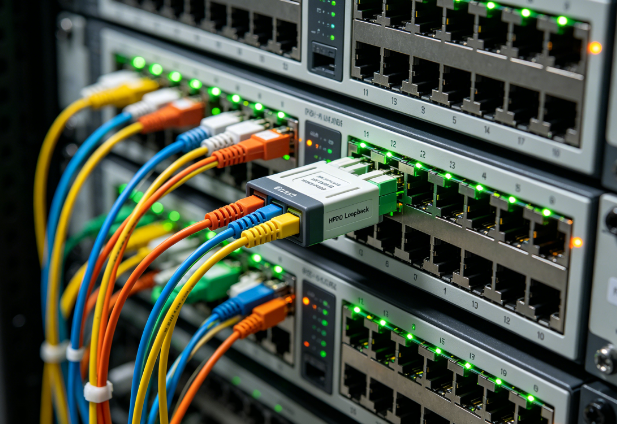
One of the most important uses of the p-type silicon wafer is in the production of integrated circuits (ICs), which form the backbone of modern electronics.
- CMOS technology foundation: P-type wafers are commonly used as substrates in complementary metal-oxide-semiconductor (CMOS) structures, which are essential for microprocessors and memory chips.
- Smart devices and computing systems: Smartphones, laptops, tablets, and wearable devices rely heavily on ICs built using p-type silicon materials.
- Signal processing and control circuits: The stable electrical properties of p-type wafers make them suitable for analog and digital circuit applications.
- Mass production efficiency: Their compatibility with large-scale manufacturing makes them ideal for consumer electronics requiring cost-effective solutions.
These applications highlight the fundamental role of p-type wafers in everyday digital technology.
Use in Solar Photovoltaic Energy Systems
The renewable energy sector is another major area where the p-type silicon wafer is widely applied, especially in solar cell production.
- Traditional solar cell base material: P-type wafers are commonly used as the base substrate in crystalline silicon photovoltaic cells.
- Efficient light absorption capability: Their material properties allow effective conversion of sunlight into electrical energy.
- Cost-effective solar panel production: Compared to alternative wafer types, p-type wafers offer lower manufacturing costs, making them suitable for large-scale solar deployment.
- Grid-connected energy systems: They are widely used in residential, commercial, and industrial solar installations around the world.
This widespread use makes p-type wafers a key contributor to global renewable energy expansion.
Industrial Electronics and Power Management Systems
Beyond consumer electronics and solar energy, the p-type silicon wafer also plays an essential role in industrial applications.
- Power control devices: Used in diodes, thyristors, and transistors that regulate electrical power in industrial systems.
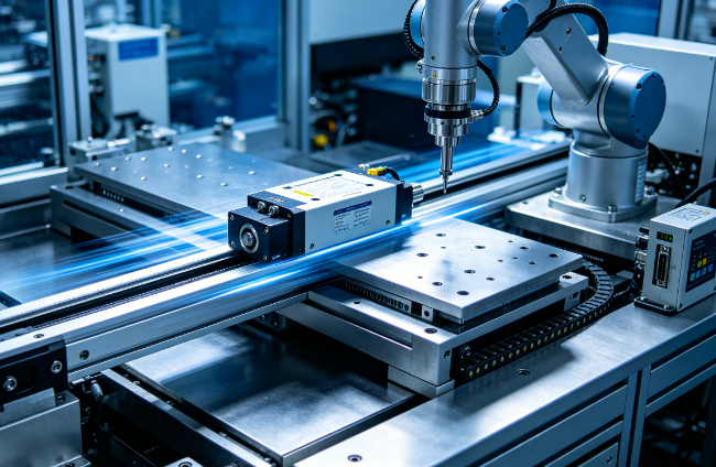
- Automation equipment: Factory automation systems rely on stable semiconductor components made from p-type wafers.
- Motor control systems: Industrial motors and drives use p-type-based components for efficient energy conversion and regulation.
- Heavy-duty electronics: Equipment used in transportation, manufacturing, and infrastructure often incorporates p-type silicon devices for reliability.
These applications demonstrate the wafer’s importance in maintaining industrial efficiency and stability.
Communication Systems and Information Technology Infrastructure
The p-type silicon wafer is also widely used in communication technologies that support global connectivity.
- Telecommunication hardware: Base stations, routers, and signal processors depend on semiconductor chips built on p-type wafers.
- Data transmission systems: Fiber optic and wireless communication equipment use integrated circuits for signal amplification and processing.
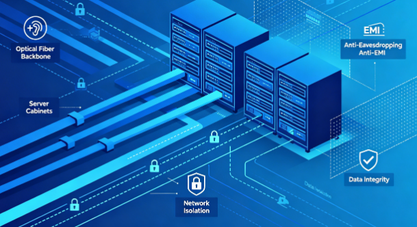
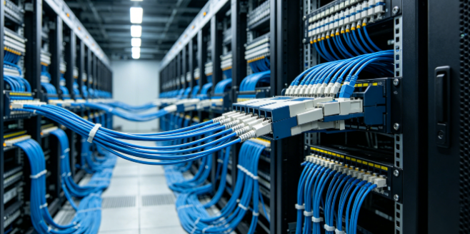
- Server and cloud infrastructure: Data centers rely on high-density semiconductor chips that often incorporate p-type silicon substrates.
- Network stability components: Power management and signal regulation circuits ensure uninterrupted communication services.
These applications make p-type wafers essential for modern digital communication networks.
Emerging Applications in Advanced Technologies
As technology continues to evolve, the p-type silicon wafer is also being integrated into emerging and advanced fields.
- Internet of Things (IoT) devices: Smart sensors and connected devices use p-type-based chips for low-cost and efficient processing.
- Medical electronics: Diagnostic equipment and monitoring systems incorporate semiconductor components for precision and reliability.
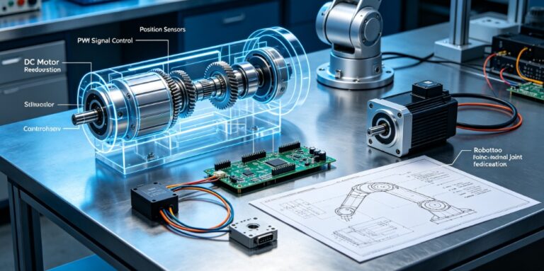
- Automotive electronics: Electric vehicles and smart cars use p-type wafers in control units and sensor systems.
- Research and development platforms: Universities and research institutions use p-type wafers in semiconductor experiments and prototyping.
These emerging applications show the continued relevance of p-type wafers in future technologies.
Conclusion
The p-type silicon wafer is widely used across modern technology, including integrated circuits, consumer electronics, solar energy systems, industrial equipment, communication infrastructure, and emerging smart technologies. Its cost efficiency, stable electrical properties, and mature manufacturing process make it a foundational material in the semiconductor industry. As technological innovation continues to expand into new fields such as IoT, automotive electronics, and renewable energy, the importance of p-type silicon wafers will remain strong, supporting the development of a more connected and energy-efficient future.
0